A PN junction diode is formed by joining two types of semiconductor materials:
- P-type semiconductor → rich in holes (positive charge carriers)
- N-type semiconductor → rich in electrons (negative charge carriers)
When these two regions are joined, a junction is formed called the PN junction.
As soon as the P and N regions are joined, electrons from the N-side diffuse into the P-side and holes from the P-side diffuse into the N-side. This results in recombination near the junction.
A region with no free charge carriers is formed near the junction, known as the depletion region. This region creates an internal electric field and a potential barrier.
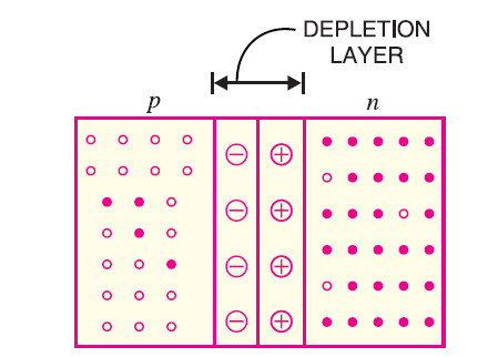
The potential barrier opposes further flow of charge carriers. Typical values are:
- Silicon diode → 0.7 V
- Germanium diode → 0.3 V
When external voltage is applied, the diode can be operated in two modes:
- Forward Bias: P-side connected to positive terminal and N-side to negative terminal.
The barrier potential decreases, depletion region narrows, and current flows easily. The diode behaves like a closed switch. - Reverse Bias: P-side connected to negative terminal and N-side to positive terminal.
The barrier potential increases, depletion region widens, and only a very small leakage current flows. The diode behaves like an open switch.
The current-voltage relationship of a diode is given by:
\[
I = I_s \left(e^{\frac{V}{\eta V_T}} – 1\right)
\]
- \(I\): Diode current
- \(I_s\): Reverse saturation current
- \(V\): Applied voltage
- \(V_T\): Thermal voltage
- \(\eta\): Ideality factor (≈ 1 to 2)
In forward bias, current increases rapidly after a certain threshold voltage. In reverse bias, only a very small current flows until breakdown occurs.