The Bipolar Junction Transistor, commonly known as the BJT, is one of the most significant inventions in the history of electronics. Before the rise of the modern Field Effect Transistor (FET), the BJT was the undisputed king of amplification and switching. Even today, it remains a cornerstone of analog circuit design due to its high gain and linearity.
Table of Contents
What is a Bipolar Junction Transistor?
A BJT is a three-terminal semiconductor device consisting of two p-n junctions. It is called “bipolar” because its operation involves both types of charge carriers: electrons and holes.
1. A transistor consists of two p-n junctions, consequently, it can be viewed as a combination of two diodes connected back-to-back.
2. The device features three terminals (the emitter, base, and collector), with each lead connected to one of the three semiconductor layers.
3. The middle section, known as the base, is fabricated as an extremely thin layer, this structural characteristic is the most critical factor enabling the transistor’s ability to control and amplify current.
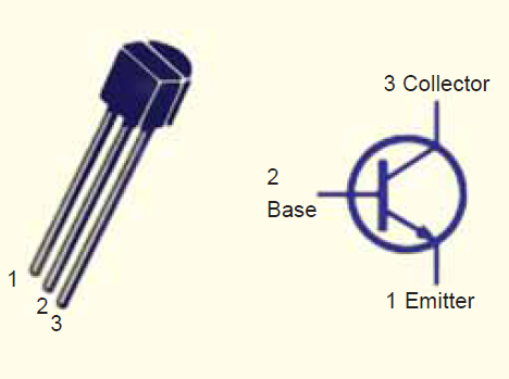
The Three Terminals
- Emitter (E): Heavily doped to emit charge carriers into the base.
- Base (B): Very thin and lightly doped; controls the flow from emitter to collector.
- Collector (C): Moderately doped and larger in size to dissipate heat.
Types of BJT: NPN vs. PNP
- NPN Transistor: A P-type layer is sandwiched between two N-type layers. Electrons are the primary charge carriers.
- PNP Transistor: An N-type layer is sandwiched between two P-type layers. Holes are the primary charge carriers.
![]()
Note: NPN transistors are preferred for high-speed applications due to higher electron mobility.
Emitter (E)
The emitter is the terminal of a Bipolar Junction Transistor (BJT) that is responsible for injecting charge carriers into the base region. It is heavily doped compared to the other regions to ensure a high concentration of carriers (electrons in NPN and holes in PNP transistors). This heavy doping allows the emitter to efficiently “emit” carriers when the base-emitter junction is forward biased. In normal operation, the emitter current ( I_E ) is the largest current in the transistor, as it supplies carriers that either recombine in the base or move toward the collector.
Base (B)
The base is the central and very thin region of the BJT, positioned between the emitter and collector. It is lightly doped and has a very small width, which plays a crucial role in transistor operation. The thinness ensures that only a small fraction of charge carriers recombine within the base, while most pass through to the collector. The base acts as a control terminal: a small base current ( I_B ) regulates a much larger collector current ( I_C ). This property is what enables the BJT to function as an amplifier, where small input signals control large output responses.
Collector (C)
The collector is the terminal that collects the charge carriers that have passed through the base region. It is moderately doped and physically larger than the emitter to handle higher power and dissipate heat effectively. The collector-base junction is typically reverse biased in active operation, creating an electric field that pulls carriers from the base into the collector. The collector current ( I_C ) forms the main output of the transistor and is largely controlled by the base current, making it essential for both amplification and switching applications.
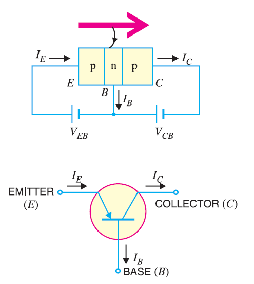
Principle of Operation (NPN)
For proper operation in the active region:
- Base-Emitter junction must be forward-biased.
- Collector-Base junction must be reverse-biased.
Only about \(1\%\) of electrons recombine in the base, while \(99\%\) reach the collector.
Current Relationship
\[
I_E = I_B + I_C
\]
- \(I_E\): Emitter current
- \(I_B\): Base current
- \(I_C\): Collector current
Key Mathematical Parameters
DC Current Gain (\(\beta\))
\[
\beta = \frac{I_C}{I_B}
\]
Typical values range from \(50\) to \(400\).
Alpha (\(\alpha\))
\[
\alpha = \frac{I_C}{I_E}
\]
Typical range: \(0.95\) to \(0.99\).
Relationship between \(\alpha\) and \(\beta\)
\[
\beta = \frac{\alpha}{1 – \alpha}
\]
Regions of Operation
| Region | BE Junction | CB Junction | Application |
|---|---|---|---|
| Cut-off | Reverse | Reverse | Off-Switch |
| Active | Forward | Reverse | Amplifier |
| Saturation | Forward | Forward | On-Switch |
| Reverse Active | Reverse | Forward | Rare |
BJT Configurations
Common Emitter (CE)
- High voltage and current gain
- Phase shift: \(180^\circ\)
Common Base (CB)
- Very low input impedance
- Very high output impedance
Common Collector (CC)
- Voltage gain: \(\approx 1\)
- High current gain
The BJT as an Amplifier
\[
V_{out} = V_{CC} – I_C R_C
\]
Since \(I_C = \beta I_B\), small input changes produce large output variations.
The BJT as a Switch
- OFF State: \(V_{BE} < 0.7V \Rightarrow I_B = 0, I_C = 0\)
- ON State: \(V_{CE(sat)} \approx 0.2V\)
Advantages and Disadvantages
Advantages
- High gain
- High-frequency operation
- Good linearity
Disadvantages
- Requires base current
- Thermal runaway risk
- Low input impedance